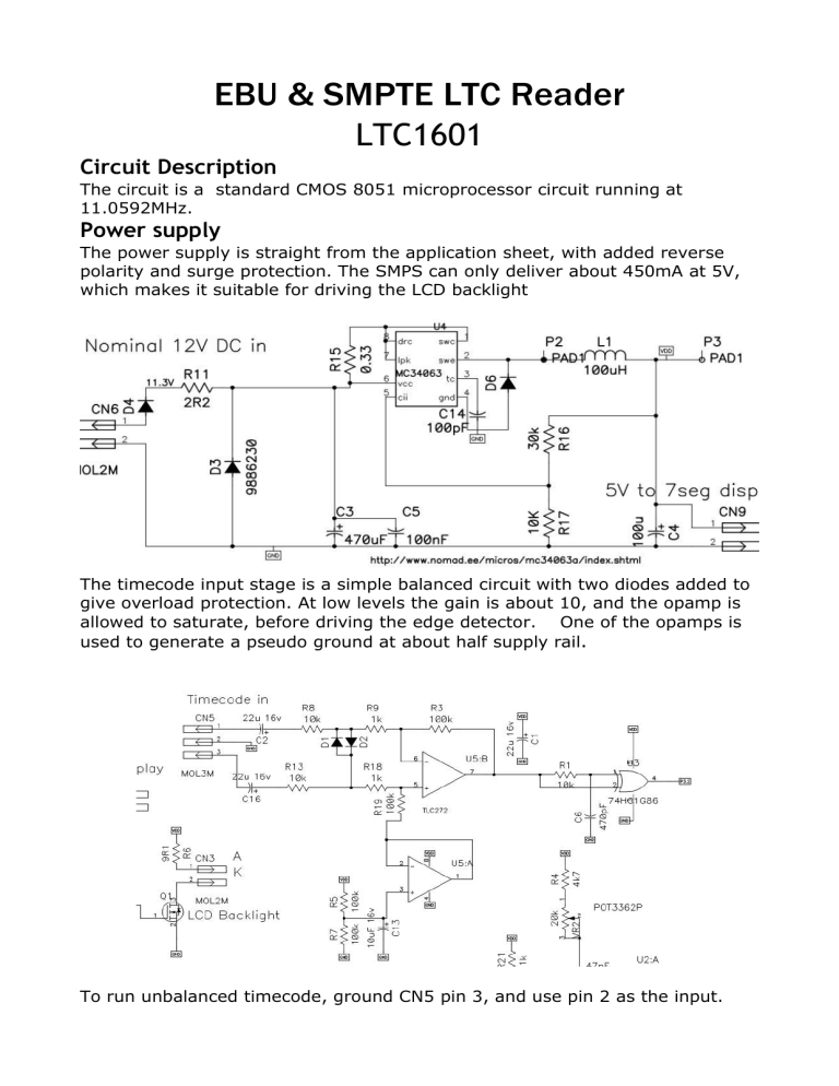
EBU & SMPTE LTC Reader LTC1601 Circuit Description The circuit is a standard CMOS 8051 microprocessor circuit running at 11.0592MHz. Power supply The power supply is straight from the application sheet, with added reverse polarity and surge protection. The SMPS can only deliver about 450mA at 5V, which makes it suitable for driving the LCD backlight The timecode input stage is a simple balanced circuit with two diodes added to give overload protection. At low levels the gain is about 10, and the opamp is allowed to saturate, before driving the edge detector. One of the opamps is used to generate a pseudo ground at about half supply rail. To run unbalanced timecode, ground CN5 pin 3, and use pin 2 as the input. The LCD control is memory mapped, taken from the Intel application brief AB39. The system will hang if programmed to use a LCD and no LCD is attached. This is because the microprocessor will be waiting for the LCD busy flag to be cleared. Timecode decoding is done in hardware, the XOR gate U3 generates positive going pulses a few microsecond wide, these go to the Int0 pin on the microprocessor, the micro will then check P3.4 to see if the monostable IC2a is running, that means a logical one has been detected, if not, a logical 0 has occurred, and the micro will trigger U2a by P3.5. This is a good point to check with a scope to see if the system is running. Timecode must be running for this to work. If no timecode is available a TTL square wave swept between 1KHz and 2.5 kHz can be used to check the circuit. Plug P1 is the factory programming connector, and is compatible with the Atmel 89s ISP interface. Once programmed P1 will be able to control the 8 digit 7 segment LED board. Data is sent serially to the display, there is no handshaking involved. The LED intensity is controlled by Pin 3 on Plug P1, normally this is pulled low by the micro and no PWM occurs. If the jumper on CN8 is changed the second monostable U2b will control the display intensity. An external pot will be required to control the display intensity. The pot should be connected between Vdd (pin5) and pin 3, but through a limiting resistor. R21 is available for this, in the PSU area of the PCB U2b is triggered by the TC clock, as it was available. This has the benefit of turning off the PWM if the TC vanishes, as it fails to a logical high so saving power. User switches CN7 is used for external switches. The switch should be wired to pull the pins 1,2,6 to ground, pin 4, the micro will provide the pullup to volts. For normal operation the switches should be open. Pins 1 and 2 have absolutely no tolerance for being pulled greater than 5V or below ground Pin 6 has diode protection and an external 10K pull up and a small capacitor. Generally, pins 1,2 should not have wires more than a few centimetres long when connection to the switches. If longer cables are required, normal ESD protection should be applied. CN7 alternate functions Pins 1 and 2 of CN7 can be programmed to act as a UART running at 9600 baud. To act as a RS232 port, a suitable line driver should be attached, MAX232 from TI and Maxim could be utilised. For the really skint operator the circuit used in the Atmel AVR Butterfly is very good. LCD backlight There is a small power Nfet on the board, Q1, this is designed to allow remote switching of the backlight. It is normally in the “on” position. To turn off the backlight, short pins 2 and 3 on CN4. CN3 is fitted to connect to the LCD. Warning the backlight is polarity sensitive. R6 limits the operating current to less that 100mA, but will not protect a reverse connected backlight. LED power The on-board SMPS can only supply about 450mA maximum to the 7Segment display, so a separate supply should be considered.

