LIDERAC – List of Equipment opened in Qualified Self - IMB-CNM
Anuncio
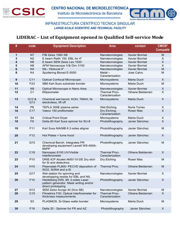
CENTRO NACIONAL DE MICROELECTRÓNICA Instituto de Microelectrónica de Barcelona INFRAESTRUCTURA CIENTÍFICO TECNICA SINGULAR LARGE-SCALE SCIENTIFIC AND TECHNICAL FACILITY LIDERAC–ListofEquipmentopenedinQualifiedSelf‐serviceMode # code Equipment Description 1 3 4 5 6 8 N7 N2 N6 N8 N4 K4 FIB Zeiss 1560 XB E beam Raith 150, EBL for 4" E beam SEM Zeiss Leo 1530 AFM Nanoacope IV& Dim 3100 NIL- Obducat 4" Sputtering Biorad E-5000 9 10 C11 F23 Optical Confocal Microscope SB6 Karl Suss substrate bonder 11 12 N9 C1 Optical Microscope in Nano Area Ellipsometer 13 Q12 & Q13 14 16 P6 C17 17 18 S4 F8 19 Area contact CMOS* Compatib Nanotecnologies Nanotecnologies Nanotecnologies Nanotecnologies Nanotecnologies Metal – Caracterization Microsystems Microsystems Xavier Borrisé Xavier Borrisé Xavier Borrisé Xavier Borrisé Xavier Borrisé Jose Calvo M X X X M M Marta Duch Marta Duch X M Nanotecnologies Thermal ProcCaracterization Microsystems Xavier Borrisé Oihane Beldarrain X X Marta Duch X Nuria Torres Roser Mas X X Critical Point Dryer Delta 80 Karl Suss spinner for SU-8 Wet Etching Dry EtchingCaracterization Microsystems Photolithography Marta Duch Javier Sánchez X X F11 Karl Suss MA/MB 6 2-sides aligner Photolithography Javier Sánchez M 20 F12 Hot Plates + fume hood Photolithography Javier Sánchez X 21 Q15 Photolithography Javier Sánchez M 22 C18 X P10 Thermal ProcCaracterization Dry Etching Oihane Beldarrain 23 Roser Mas M 24 H10 Thermal Proc. Oihane Beldarrain M 25 Q17 Nanotecnologies Xavier Borrisé X 26 F10 Photolithography Javier Sánchez X 27 28 N12 C15 Chemical Bench. Integrates PR developing equipment Laurell WS-400A6NPP Nanospec 6100 UV/Visible interferometer DRIE-ICP Alcatel AMS110-DE Dry etch for Si and dielectrics Plasmalab PL800- PECVD deposition of SiO2, Si3N4 and a-Si Wet station for spinning and developping resists for EBL and NIL Heidelberg DWL 99: 2-sides Laser pattern generator. Mask writing and/or direct prototyping SEM Zeiss Auriga 40 (fora SB) Filmetrics F20. Optical interforemeter for thickness measurements Nanotecnologies Thermal ProcCaracterization Xavier Borrisé Oihane Beldarrain M X 29 S3 PLASMOS. Si-Glass wafer bonder Microsystems Marta Duch M 30 F19 Delta 20 - Spinner for FR and AZ Chemical wet bench: KOH, TMAH, Ni electroless, lift off TEPLA 300E plasma asher Veeco 150 profilometer Photolithography Javier Sánchez X CENTRO NACIONAL DE MICROELECTRÓNICA Instituto de Microelectrónica de Barcelona INFRAESTRUCTURA CIENTÍFICO TECNICA SINGULAR LARGE-SCALE SCIENTIFIC AND TECHNICAL FACILITY (*) Note: The Clean Room has a CMOS technology acting as a reference, so that appropriate cleaning and contamination‐free conditions must be observed. The same applies to a set of other CMOS‐compatible or CMOS‐like existing technologies. Therefore potential risks of contamination of equipment, tools and environment must be avoided. Those risks are basically of two types: a) alkali metal ions (Na, K) and b) contaminant metals like some noble metals (Au, Pt, Pd, Ag) that are almost impossible to remove by conventional cleaning processes used in the Cleanroom. The most critical systems from this point of view are the oxidation‐diffusion furnaces. Related to contamination of the equipment 3 levels are identified: a) clean systems (C): only CMOS‐technology‐compatible samples can be processed. b) MNC Equipment (M): contaminated samples (for instance with noble metals contents) can be processed. c) Mixed systems (X): systems that can be considered as clean or as MNC, depending on the appropriate use of some accessories.
